Providing a vast array of electronic components, sensors and connectors for all types of applications and industries
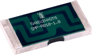
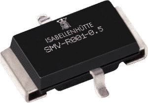
Precision and power resistors for aerospace applications
Highest reliability and 100% traceability
ESCC 4001/027 and ESCC 4001/028 qualified parts


Shop by category
Shop by approval

About Rhopoint Components
As a member of the Rhopoint Group, Rhopoint Components is a professional distributor of precision electronic components, sensors and connectors. As an authorised partner of 28 industry-leading manufacturers around the world,u00a0 we have met the high requirements of the UK and international markets since 1975.
Our friendly and professional team provides you with the highest-level technical and logistical support. We provide fully customised solutions to meet your specific technical requirements. In addition, a large number of standard products are also available in our inventory. All of this is due to our efficient sales and distribution operations at our headquarters in Sussex. Our offices and field engineers throughout the UK and Europe will be happy to advise you and provide you with the best possible solutions. We are happy to discuss your request or enquiries via phone, email, live chat or face to face and look forward to meeting you.


